-
 English
 -
 简体中文
简体中文


Categories
- Laser
-
Light source
- Laser diode
- laser Source
- Benchtop ASE Light Source
- SLD model
- SLD light source
- Visible Fiber Lasers
- Erbium Broadband Sources-Dual Band
- Raman Fiber Amplifiers
- Micro Broadband Source
- Benchtop EDFA
- S-band Optical Amplifier (TDFA)
- ASBN-D130/230 deep UV Deuterium Light Source Assembly
- ASB-XE-175 Xenon Fiber Optic Light Source
- ASC Series Spectral Calibration Lamps and Assemblies
- AST/ASTN series wavelength tunable light sources
- ASBN-W High power Tungsten-Halogen Light Source Series
- Picosecond
- ASBN-DW-MINI Miniature hybrid light source
- optical fiber amplifier
- Multi line laser
- Laser detection
- Information optics
- Fiber compenent
- Laser Crystal
- Laser modulation
- Laser imaging
- Laser Components
- Fiber Fused Biconic Tapering System
- Instrument
- Optics
- 2um Fiber compenent
- Optomechanics
- Lab Consumable
- Optical fiber testing instrument
- agent
Solution
- 光纤激光器的工作原理及其发展前景
- 激光切割异型工作的难点分析
- 光学斩波器及原理
- 空间应用的紫外激光器寿命论证
- wavelength-division-multiplexers
- 拉曼光纤放大器
- Introduction to Fluorescence Filters
- General Introduction to Raman Spectroscopy
- How does a SAM™ work ?
- 激光干涉仪常见故障处理方法
- 盘点光纤传感器四十年发展史
- 空间光调制器简介及其应用
- 什么是空间光调制器
- THz 技术及其应用
- 光学相干断层扫描技术
- Four-Point Probes and Resistivity Testing Equipment
- Infrared Spectroscopy
- AO-OCT Comes into Focus
PRODUCTS
- Thorlabs optoelectronic products agents
- Spectralproducts
- Nethis
- Protemics GmbH
- andover Filters
- Eksma Optics
- EKSPLA
- optical passive components
- Schafter+Kirchhoff
- Electrophysics
- electrooptic IR VIEWERS products
- ALPHALAS DPSS Lasers
- QPhotonics
- Superlum products
- edmund products
- sartorius products
- Tydex Tera Hertz products
- Wasatch Photonics products
- Optromix Company
- About Best Scientific
- Qontrol Systems LLP
- HQ Graphene High Quality 2D Crystals
- iXblue intensity modulators
- Newlight Photonics
Technical document
- Machine Vision
- Optical CoherenceTomography
- Terahertz
- Photoelectric detection technology
- Optical fiber device
- Photodiode Tutorial
- Optical industry and photography industry common English abbreviations
- 高精度纯相位液晶空间光调制器的研究
- 中国计划建造全球最大直径射电望远镜
- spectrometers
- Light source / xenon lamp / mercury lamp light source
- Laser Range Finders
- 激光冷却的原理和技术进展
- Research of the phase-only modulation characterization of a liquid crystal spatial light modulator
- 基于空间光调制器的飞秒激光并行加工技术研究
- Research of Fresnel Incoherent Correlation Digital Holography Based on SLM
- 【Thorlabs教程】氦氖激光器
- OCT Image Gallery
- 光学滤光片的作用原理及应用
- 半导体泵浦与灯泵浦激光器在打标上的对比
- 如何选取激光功率计和能量计
- 液晶空间光调制器的研究
- Thorlabs太赫兹教程
- 【Thorlabs教程】激光扫描显微镜
- Principle of spatial light modulator
- 光隔离器介绍
- Survey on Methods and Systems of Color Holographic Display
- Progress on the terahertz wave radiation properties of Photoconductive Antenna
- 光无源器件(optical passive components)种类及原理
- The main functions of spatial light modulator
How does a SAM™ work ?
|
How does a SAM™ work ?
|
|||||||||||||||||||||||||||||||||||||||||||||||||||||||||||||||||||||||||||||||||||||||||||||||||||||||||
| Contents | |||||||||||||||||||||||||||||||||||||||||||||||||||||||||||||||||||||||||||||||||||||||||||||||||||||||||
| > | 1. Aim of SAM | ||||||||||||||||||||||||||||||||||||||||||||||||||||||||||||||||||||||||||||||||||||||||||||||||||||||||
|
Passive mode-locking techniques for the generation of ultra-short pulse trains are preferred over active techniques due to the ease of incorporation of passive devices into various laser cavities. |
|||||||||||||||||||||||||||||||||||||||||||||||||||||||||||||||||||||||||||||||||||||||||||||||||||||||||
| > | 2. Parameters | ||||||||||||||||||||||||||||||||||||||||||||||||||||||||||||||||||||||||||||||||||||||||||||||||||||||||
|
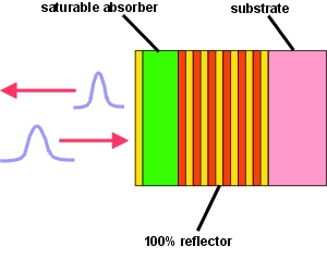
A SAM consists of a Bragg-mirror on a semiconductor wafer like GaAs, covered by an absorber layer and a more or less sophisticated top film system, determining the absorption. |
|||||||||||||||||||||||||||||||||||||||||||||||||||||||||||||||||||||||||||||||||||||||||||||||||||||||||
| > | 3. Absorption | ||||||||||||||||||||||||||||||||||||||||||||||||||||||||||||||||||||||||||||||||||||||||||||||||||||||||
| A SAM is a nonlinear optical device. Therefore the absorption A1 depends on the pulse fluence F. If the pulse duration τp is shorter than the relaxation time τ of the absorber material, then the fluence dependent absorption is given by | |||||||||||||||||||||||||||||||||||||||||||||||||||||||||||||||||||||||||||||||||||||||||||||||||||||||||
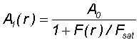 |
with | 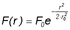 |
eq. (1) | ||||||||||||||||||||||||||||||||||||||||||||||||||||||||||||||||||||||||||||||||||||||||||||||||||||||
| A0 | small signal saturable absorption | ||||||||||||||||||||||||||||||||||||||||||||||||||||||||||||||||||||||||||||||||||||||||||||||||||||||||
| F(r) | radial dependent fluence of a Gaussian pulse | ||||||||||||||||||||||||||||||||||||||||||||||||||||||||||||||||||||||||||||||||||||||||||||||||||||||||
| Fsat | saturation fluence of the absorber material | ||||||||||||||||||||||||||||||||||||||||||||||||||||||||||||||||||||||||||||||||||||||||||||||||||||||||
| F0 | average value of the pulse fluence | ||||||||||||||||||||||||||||||||||||||||||||||||||||||||||||||||||||||||||||||||||||||||||||||||||||||||
| r | radius, distance from the beam axis | ||||||||||||||||||||||||||||||||||||||||||||||||||||||||||||||||||||||||||||||||||||||||||||||||||||||||
| r0 | Gaussian beam radius | ||||||||||||||||||||||||||||||||||||||||||||||||||||||||||||||||||||||||||||||||||||||||||||||||||||||||
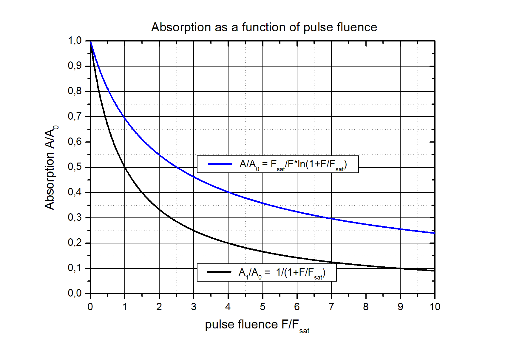
| The effective absorption A of a Gaussian beam is the result of an averaging over the radial dependent fluence F(r) of the pulse: | |||||||||||||||||||||||||||||||||||||||||||||||||||||||||||||||||||||||||||||||||||||||||||||||||||||||||
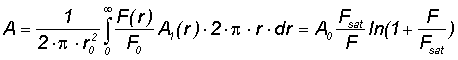 |
eq. (2) | ||||||||||||||||||||||||||||||||||||||||||||||||||||||||||||||||||||||||||||||||||||||||||||||||||||||||
| In the figure below the saturation of the absorption according to equations (1) and (2) (blue curve) is shown. For small fluence F < Fsat the absorption drops down linear with increasing fluence | |||||||||||||||||||||||||||||||||||||||||||||||||||||||||||||||||||||||||||||||||||||||||||||||||||||||||
 |
|||||||||||||||||||||||||||||||||||||||||||||||||||||||||||||||||||||||||||||||||||||||||||||||||||||||||
|
The small signal absorption A0 is proportional to the square of the electric field strength of the standing wave at the position of the absorber layer. Therefore the saturable absorption of the SAM can be adjusted by the design. A typical value for the saturation fluence Fsat is 50 µJ/cm2. |
|||||||||||||||||||||||||||||||||||||||||||||||||||||||||||||||||||||||||||||||||||||||||||||||||||||||||
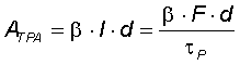
| For short pulses the two-photon absorption ATPA increases the total absorption as follows: | |||||||||||||||||||||||||||||||||||||||||||||||||||||||||||||||||||||||||||||||||||||||||||||||||||||||||
 |
eq. (3) | ||||||||||||||||||||||||||||||||||||||||||||||||||||||||||||||||||||||||||||||||||||||||||||||||||||||||
| with | β | two-photon absorption coefficient | |||||||||||||||||||||||||||||||||||||||||||||||||||||||||||||||||||||||||||||||||||||||||||||||||||||||
| I | pulse intensity | ||||||||||||||||||||||||||||||||||||||||||||||||||||||||||||||||||||||||||||||||||||||||||||||||||||||||
| d | thickness of the absorber layer | ||||||||||||||||||||||||||||||||||||||||||||||||||||||||||||||||||||||||||||||||||||||||||||||||||||||||
| F | pulse fluence | ||||||||||||||||||||||||||||||||||||||||||||||||||||||||||||||||||||||||||||||||||||||||||||||||||||||||
| τP | pulse duration | ||||||||||||||||||||||||||||||||||||||||||||||||||||||||||||||||||||||||||||||||||||||||||||||||||||||||
| > | 4. Modulation depth ΔR | ||||||||||||||||||||||||||||||||||||||||||||||||||||||||||||||||||||||||||||||||||||||||||||||||||||||||
|
The reflectance R of a saturable absorber mirror (SAM) is in the region of the stop-band with zero transmittance determined by the absorption A according to R = 1-A. The modulation depth ΔR is smaller than the absorption A0 because of non-saturable losses Ans: ΔR = A0 -Ans. The main reason for the non-saturable losses are crystal defects, which are needed for fast relaxation of the excited carriers. The modulation depth increases with increasing relaxation time t. Typical values for ΔR are
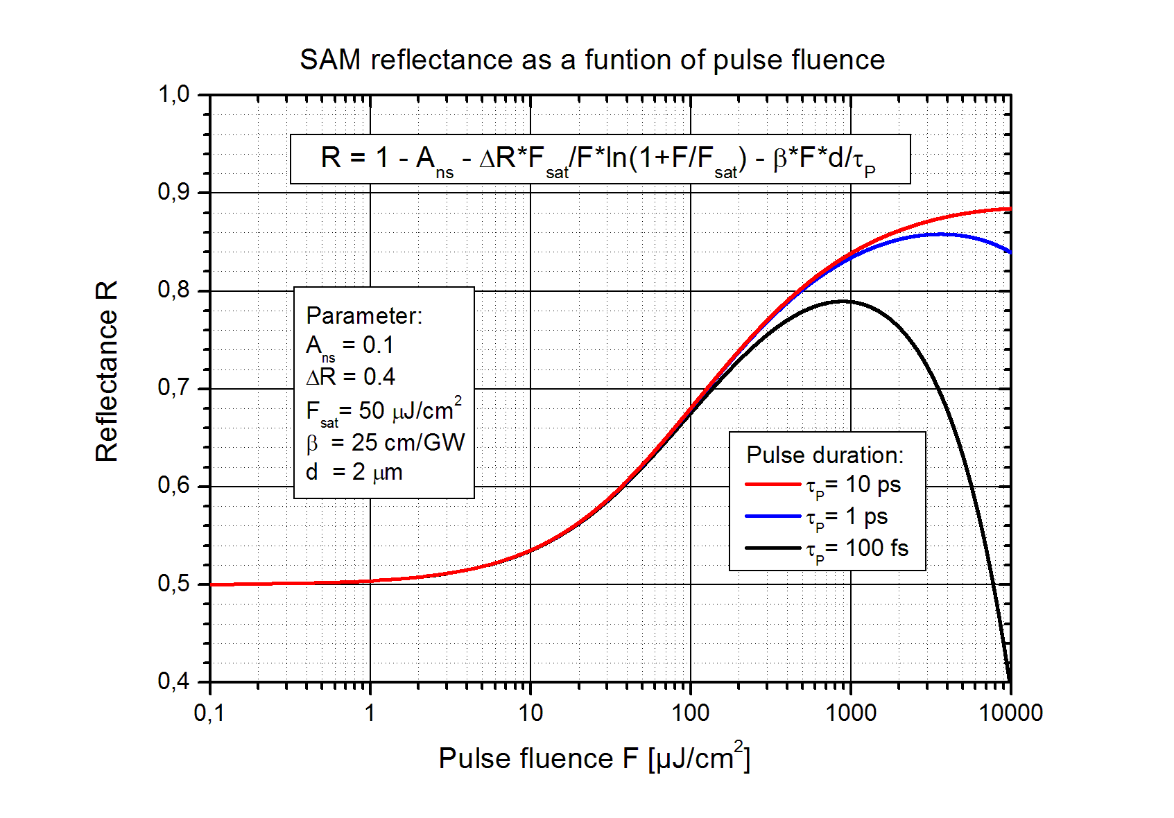
The pulse fluence dependent reflection R(F) of a saturable absorber mirror is governed by the effective absorption according to eq.(2). For short pulses and high pulse intensities I the two photon absorption decreases the reflection and therefore also the effective modulation depth according to eq.(3). Therefore the reflectance R of a SAM can be written as |
|||||||||||||||||||||||||||||||||||||||||||||||||||||||||||||||||||||||||||||||||||||||||||||||||||||||||
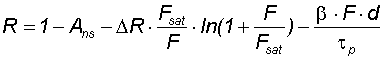 |
eq. (4) | ||||||||||||||||||||||||||||||||||||||||||||||||||||||||||||||||||||||||||||||||||||||||||||||||||||||||
| The calculated SAM reflectance R as a function of pulse fluence F according to eq. (4) is shown for three different pulse durations in the figure below. | |||||||||||||||||||||||||||||||||||||||||||||||||||||||||||||||||||||||||||||||||||||||||||||||||||||||||
 |
|||||||||||||||||||||||||||||||||||||||||||||||||||||||||||||||||||||||||||||||||||||||||||||||||||||||||
| > | 5. Relaxation time | ||||||||||||||||||||||||||||||||||||||||||||||||||||||||||||||||||||||||||||||||||||||||||||||||||||||||
|
The saturable absorber layer consists of a semiconductor material with a direct band gap slightly lower than the photon energy. During the absorption electron-hole pairs are created in the film. The relaxation time t of the carriers has to be a little bit longer than the pulse duration. In this case the back side of the pulse is still free of absorption, but during the whole period between two consecutive pulses the absorber is non saturated and prevents Q-switched mode-locking of the laser.
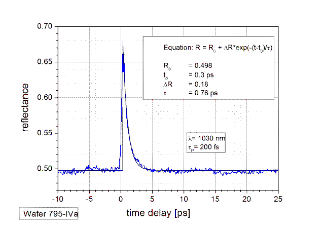
The parameters to adjust the relaxation time in both technologies are the growth temperature in case of LT-MBE and the ion dose in case of implantation. Typical values of the relaxation time t of SAMs are between 500 fs and 10 ps. An example of a pump-probe measurement to determine the relaxation time τ is shown below. |
|||||||||||||||||||||||||||||||||||||||||||||||||||||||||||||||||||||||||||||||||||||||||||||||||||||||||
 |
|||||||||||||||||||||||||||||||||||||||||||||||||||||||||||||||||||||||||||||||||||||||||||||||||||||||||
| > | 6. Saturation fluence Fsat | ||||||||||||||||||||||||||||||||||||||||||||||||||||||||||||||||||||||||||||||||||||||||||||||||||||||||
|
The saturation fluence depends on the semiconductor material parameters and on the optical design of the SAM. To prevent the SAM from unwanted degradation and destruction due to high pulse fluences, the saturation fluence must be low. |
|||||||||||||||||||||||||||||||||||||||||||||||||||||||||||||||||||||||||||||||||||||||||||||||||||||||||
| > | 7. Absorber temperature | ||||||||||||||||||||||||||||||||||||||||||||||||||||||||||||||||||||||||||||||||||||||||||||||||||||||||
|
The saturable absorber converts a part of the incoming photon energy into heat. This thermal energy increases the absorber layer temperature during and shortly after an optical pulse. After that the heat is transported through the substrate to the heat sink on the rear substrate side. In case of a substrate like GaAs with a high thermal conductivity only a negligible amount of the dissipated heat goes trough the front surface of the absorber into air. |
|||||||||||||||||||||||||||||||||||||||||||||||||||||||||||||||||||||||||||||||||||||||||||||||||||||||||
 |
eq. (5) | ||||||||||||||||||||||||||||||||||||||||||||||||||||||||||||||||||||||||||||||||||||||||||||||||||||||||
|
If the laser spot radius r on the absorber surface is small in comparison to the substrate thickness (typically 0.5 mm) then the heat flow in the absorber layer is nearly one dimensional but in the substrate three dimensional (with a point source). Then the heat is distributed into a half space of the substrate resulting in a temperature field with nearly concentric interfaces of equal temperature. |
|||||||||||||||||||||||||||||||||||||||||||||||||||||||||||||||||||||||||||||||||||||||||||||||||||||||||
 |
eq. (6) | ||||||||||||||||||||||||||||||||||||||||||||||||||||||||||||||||||||||||||||||||||||||||||||||||||||||||
|
Here λ is the thermal conductivity, ri is the inner (illuminated) radius of a sphere and ro an outer radius of a sphere with the heat sink temperature T0. The approximation used is ri « ro when we consider the GaAs wafer thickness as ro substantial larger then the laser spot radius ri=r. The mean absorbed optical power is |
|||||||||||||||||||||||||||||||||||||||||||||||||||||||||||||||||||||||||||||||||||||||||||||||||||||||||
| eq. (7) | |||||||||||||||||||||||||||||||||||||||||||||||||||||||||||||||||||||||||||||||||||||||||||||||||||||||||
|
To take into account that the heat flow is only into a half space (not to air) and that in the vicinity of the absorber layer the flow is nearly one dimensional (not three dimensional as calculated) the real temperature rise is about by a factor of 4 higher then in the above formula (6), so that |
|||||||||||||||||||||||||||||||||||||||||||||||||||||||||||||||||||||||||||||||||||||||||||||||||||||||||
 |
eq. (8) | ||||||||||||||||||||||||||||||||||||||||||||||||||||||||||||||||||||||||||||||||||||||||||||||||||||||||
|
If the laser spot radius r is larger then the substrate thickness d then the heat flow is nearly one dimensional and then r must be replaced by d in the above equation (8). |
|||||||||||||||||||||||||||||||||||||||||||||||||||||||||||||||||||||||||||||||||||||||||||||||||||||||||
 |
eq. (9) | ||||||||||||||||||||||||||||||||||||||||||||||||||||||||||||||||||||||||||||||||||||||||||||||||||||||||
|
Here the heated volume after the laser pulse is approximated by the product of the illuminated area and the diffusion length (4at)1/2. |
|||||||||||||||||||||||||||||||||||||||||||||||||||||||||||||||||||||||||||||||||||||||||||||||||||||||||
 |
eq. (10) | ||||||||||||||||||||||||||||||||||||||||||||||||||||||||||||||||||||||||||||||||||||||||||||||||||||||||
|
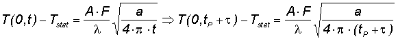
The maximum total absorber temperature increase ΔTmax can be described by the sum of the time dependent dynamical part ΔTdyn(τ+tp) and the static part ΔTstat. |
|||||||||||||||||||||||||||||||||||||||||||||||||||||||||||||||||||||||||||||||||||||||||||||||||||||||||
 |
eq. (11) | ||||||||||||||||||||||||||||||||||||||||||||||||||||||||||||||||||||||||||||||||||||||||||||||||||||||||
| with | ΔT | temperature rise | |||||||||||||||||||||||||||||||||||||||||||||||||||||||||||||||||||||||||||||||||||||||||||||||||||||||
| A | absorption | ||||||||||||||||||||||||||||||||||||||||||||||||||||||||||||||||||||||||||||||||||||||||||||||||||||||||
| F | pulse fluence | ||||||||||||||||||||||||||||||||||||||||||||||||||||||||||||||||||||||||||||||||||||||||||||||||||||||||
| λth | thermal conductivity of the absorber material (55 W/(mK) for GaAs) | ||||||||||||||||||||||||||||||||||||||||||||||||||||||||||||||||||||||||||||||||||||||||||||||||||||||||
| a | thermal diffusivity of the absorber material (3.1 10-5 m2/s for GaAs) | ||||||||||||||||||||||||||||||||||||||||||||||||||||||||||||||||||||||||||||||||||||||||||||||||||||||||
| tp | optical pulse duration | ||||||||||||||||||||||||||||||||||||||||||||||||||||||||||||||||||||||||||||||||||||||||||||||||||||||||
| τ | carrier relaxation time in the absorber | ||||||||||||||||||||||||||||||||||||||||||||||||||||||||||||||||||||||||||||||||||||||||||||||||||||||||
| r | spot radius on the absorber | ||||||||||||||||||||||||||||||||||||||||||||||||||||||||||||||||||||||||||||||||||||||||||||||||||||||||
| f | optical pulse repetition rate | ||||||||||||||||||||||||||||||||||||||||||||||||||||||||||||||||||||||||||||||||||||||||||||||||||||||||
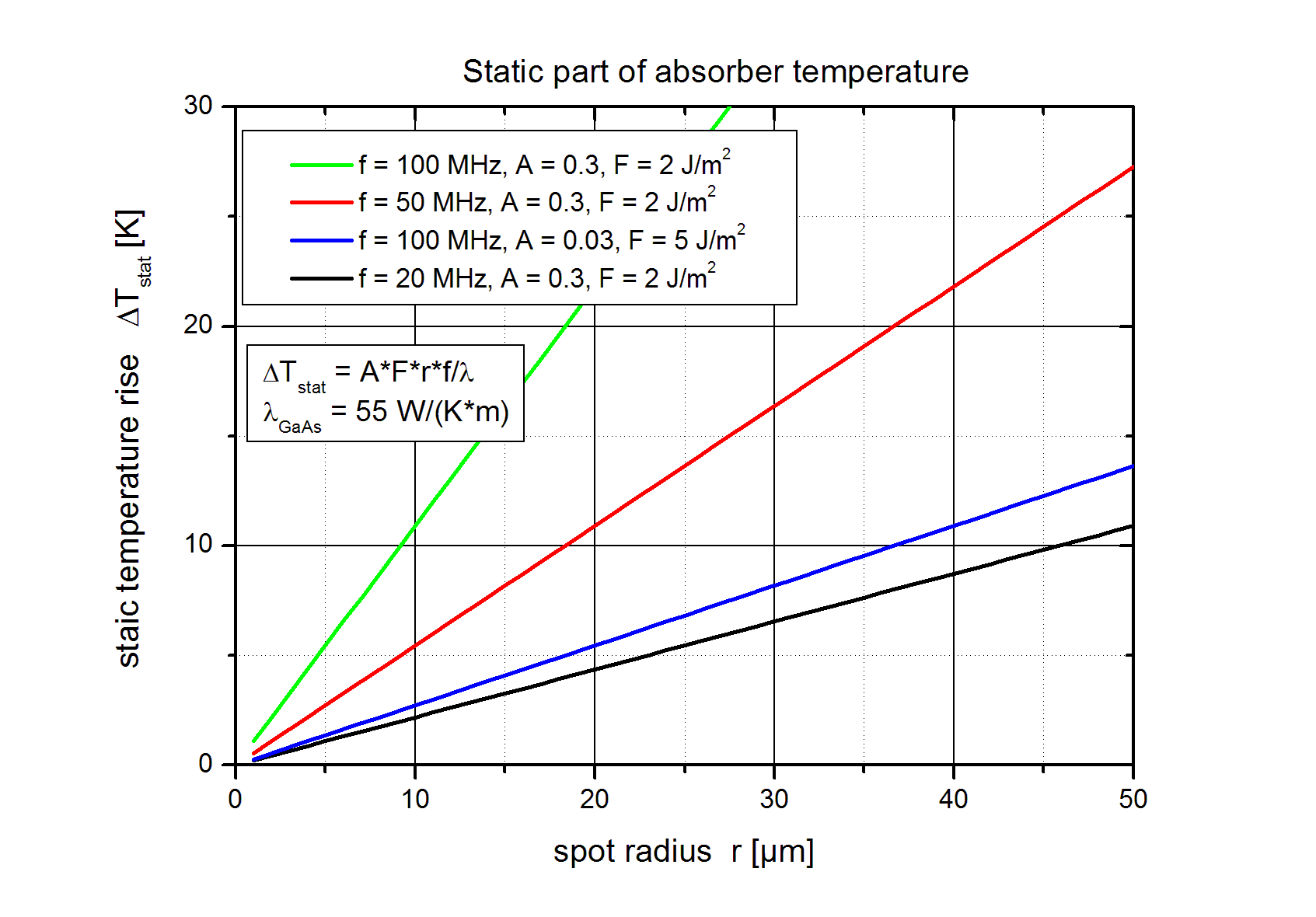
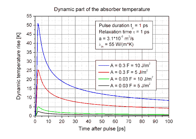
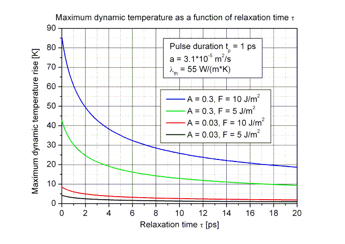
| The two figures below show the static temperature rise ΔTstat as a function of the optical spot radius r and the dynamic temperature rise ΔTdyn as a function of the absorber relaxation time for typical parameters in solid state (absorption A = 0.03) and fiber lasers (absorption A = 0.3) according to eqs. (9) and (11). | |||||||||||||||||||||||||||||||||||||||||||||||||||||||||||||||||||||||||||||||||||||||||||||||||||||||||
 |
|||||||||||||||||||||||||||||||||||||||||||||||||||||||||||||||||||||||||||||||||||||||||||||||||||||||||
 |
|||||||||||||||||||||||||||||||||||||||||||||||||||||||||||||||||||||||||||||||||||||||||||||||||||||||||
| The maximum temperature rise decreases with increasing absorber relaxation time τ because the absorbed energy is released from the excited electrons into the crystal lattice after the relaxation time. If the relaxation time τ is longer then the pulse duration tp the electrons store the absorbed energy for a short time whereas the thermal energy diffuse already from the absorber layer into the substrate. | |||||||||||||||||||||||||||||||||||||||||||||||||||||||||||||||||||||||||||||||||||||||||||||||||||||||||
 |
|||||||||||||||||||||||||||||||||||||||||||||||||||||||||||||||||||||||||||||||||||||||||||||||||||||||||
| > | 8. Reflection and absorption bandwidth | ||||||||||||||||||||||||||||||||||||||||||||||||||||||||||||||||||||||||||||||||||||||||||||||||||||||||
| 7.1 Time-bandwidth product (TBWP) | |||||||||||||||||||||||||||||||||||||||||||||||||||||||||||||||||||||||||||||||||||||||||||||||||||||||||
From Heisenberg's uncertainty principle for the conjugated variables pulse width Δt and photon energy E = hν the TBWP of a laser pulse is limited to about Δt.Δν ≥ 1/(2π).
The minimum TBWP for a Sech2pulse is Δt.Δν = 0.32 . Most people do not work with frequency ν but prefer wavelength λ. Using the relation c=λ.ν the frequency interval Δν is related to the wavelength interval Δλ by Δν = - c. Δλ/λ2. c = 2.988 . 108 m/s is the speed of light in the vacuum. |
|||||||||||||||||||||||||||||||||||||||||||||||||||||||||||||||||||||||||||||||||||||||||||||||||||||||||
| Numerical values for the minimum bandwidth Δν as a function of pulse duration Δt | |||||||||||||||||||||||||||||||||||||||||||||||||||||||||||||||||||||||||||||||||||||||||||||||||||||||||
|
|||||||||||||||||||||||||||||||||||||||||||||||||||||||||||||||||||||||||||||||||||||||||||||||||||||||||
| Numerical values for the minimum bandwidth in nm as a function of pulse duration Δt | |||||||||||||||||||||||||||||||||||||||||||||||||||||||||||||||||||||||||||||||||||||||||||||||||||||||||
|
|||||||||||||||||||||||||||||||||||||||||||||||||||||||||||||||||||||||||||||||||||||||||||||||||||||||||
| 7.2 Reflection bandwidth | |||||||||||||||||||||||||||||||||||||||||||||||||||||||||||||||||||||||||||||||||||||||||||||||||||||||||
|
The reflection bandwidth of the SAM has to be larger than the pulse bandwidth. In case of a SAM with an underlying Bragg-mirror the reflection bandwidth is determined by the ratio of the refractive indices nH/nL of the layers in the thin film stack. More about Bragg-mirrors ... |
|||||||||||||||||||||||||||||||||||||||||||||||||||||||||||||||||||||||||||||||||||||||||||||||||||||||||
| 7.3 Absorption bandwidth | |||||||||||||||||||||||||||||||||||||||||||||||||||||||||||||||||||||||||||||||||||||||||||||||||||||||||
|
An ideal SAM has a constant saturable absorption for all wavelengths of the pulse spectrum. Because of the wavelength dependence of the absorption in a semiconductor material above the band gap, the absorption increases with decreasing wavelength. In case of a resonant SAM this dependency may be changed by the standing waves inside the cavity in such a way, that the maximum absorption is at the resonance wavelength of the SAM. |
|||||||||||||||||||||||||||||||||||||||||||||||||||||||||||||||||||||||||||||||||||||||||||||||||||||||||